
If you are reading this on a phone, a laptop, or even a tablet mounted to your kitchen wall, you are currently holding millions of tiny, invisible silicon gates. Most of us rarely think about semiconductor hardware during our daily routine. We tap a screen, expect an app to load instantly, and get annoyed if a video buffers for more than two seconds.
Yet behind every single digital interaction lies a physical piece of silicon working exceptionally hard.
As we navigate 2026, the chip industry is going through its most drastic transformation in decades. For nearly half a century, the golden rule of tech was simple: make transistors smaller, pack more of them onto a single piece of silicon, and watch computing power skyrocket while prices drop. Engineers call this relentless pursuit Moore’s Law.
However, physics is finally hitting a brick wall. We are now manufacturing components at scale so absurdly small that electrons start behaving strangely and jumping across barriers where they should not. Simply shrinking things down is no longer enough.
At the exact same time, the massive global explosion in artificial intelligence has created an insatiable appetite for raw computing power and memory speed. Data centers are burning through electricity, supply chains are stretched thin, and tech companies are realizing that the old ways of building processors simply cannot keep up.
So, what is actually happening under the hood of modern technology? Let us strip away the confusing corporate jargon and look at how chips are really being built today, why it matters for your everyday devices, and where this multi-trillion-dollar industry is heading next.
What Is Semiconductor Hardware, Really?
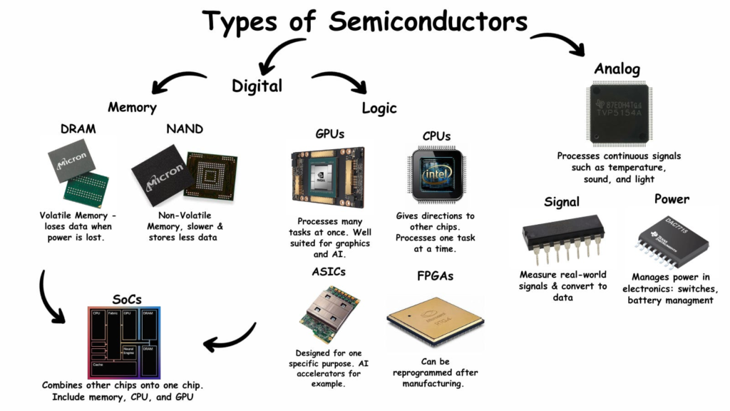
To understand why the tech world is practically obsessing over silicon right now, it helps to step back and look at what a semiconductor actually does.
In basic terms, a semiconductor is a material that sits right in the middle of being a great conductor of electricity (like copper) and a total insulator (like rubber). Silicon, which comes from purified sand, happens to be the undisputed king of these materials.
By carefully treating silicon with tiny amounts of other elements, engineers can create billions of microscopic switches called transistors.
                                  HOW A TRANSISTOR WORKS

                                    [ Control Gate ]
                                           │
                                           ▼
            [ Source ]  ───────►  [ Silicon Channel ]  ───────►  [ Drain ]
                                  (Current Flows or Stops)
Think of a transistor as an light switch, except instead of flipping it with your thumb, it flips electronically billions of times per second.
- When the switch is ON, electricity flows (representing a 1 in digital code).
- When the switch is OFF, electricity stops (representing a 0 in digital code).
Every photo you take, every video you stream, every email you send, and every AI prompt you run boils down to billions of these tiny switches turning on and off in precise patterns. When your phone opens a camera app instantly, or your car predicts a lane drift using sensors, semiconductor hardware is carrying the entire physical workload behind the curtain.
The Big Shift: Why 2026 Is Different

For decades, the standard playbook for chipmakers like Intel, TSMC, and Samsung was straightforward: upgrade the manufacturing equipment, shrink the silicon node, and print a bigger, faster single block of silicon (known in the industry as a monolithic die).
That approach is officially running out of steam.
Making a giant single chip at ultra-tiny manufacturing nodes is becoming ridiculously expensive. Worse yet, if a single microscopic defect occurs on a massive silicon wafer during manufacturing, the entire chip often has to be thrown away. As chips get larger, yield rates drop, and costs skyrocket out of control.
                    OLD MONOLITHIC CHIP vs. MODERN CHIPLET SYSTEM

        ┌─────────────────────────┐               ┌─────────────────────────┐
        │                         │               │  [CPU]     │    [GPU]   │
        │   ONE GIANT DIE         │               │ ───────────┼─────────── │
        │   (High failure rate,   │      VS.      │  [Memory]  │   [I/O]    │
        │    extremely expensive) │               │ ─────────────────────── │
        │                         │               │  INTERPOSER / BASE DIE  │
        └─────────────────────────┘               └─────────────────────────┘
Furthermore, generative AI models have flipped traditional computing priorities on their head. Standard processors spend a lot of time waiting around for data to travel back and forth from separate storage drives. AI workloads, on the other hand, require thousands of operations running simultaneously across massive datasets.
The industry is no longer just asking, “How do we squeeze more transistors onto this piece of silicon?” Today, the primary question is, “How do we stitch multiple specialized components together so data moves faster without melting the power grid?”
Real-World Comparison: The Silicon Tech Landscape
To make sense of all the terms floating around news headlines today, here is a breakdown of how the key engineering approaches compare in terms of real-world impact, cost, and practical utility.
| Innovation Area | What It Actually Does | Why Engineers Care | Real-World Impact | Primary Limitation |
|---|---|---|---|---|
| Specialized AI Chips | Processes massive parallel calculations instead of sequential tasks | Delivers raw mathematical throughput for complex models | Powers fast voice assistants, real-time translation, and image tools | Consumes huge amounts of electrical power and generates intense heat |
| Chiplet Architectures | Breaks a big processor into smaller, specialized silicon blocks | Reduces manufacturing waste and allows mixing different production nodes | Keeps high-end computers and servers affordable | Requires complex internal wiring and precise software integration |
| Advanced Packaging | Connects separate chips side-by-side or stacked on a shared base | Reduces physical distance between components to speed up data | Enables thinner devices with desktop-class performance | Extremely difficult to manufacture without high failure rates |
| High-Bandwidth Memory | Stacks memory chips vertically directly next to the main processor | Eliminates data bottlenecks by providing massive pipeline widths | Prevents AI applications from freezing or slowing down during heavy tasks | Extremely expensive and currently in short global supply |
| 3D Integration | Stacks logic directly on top of logic or memory vertically | Drastically shortens physical distances electricity must travel | Fits extreme computing power into tiny, compact form factors | Traps thermal heat between layers, making cooling a massive headache |
| Custom Silicon | Purpose-built chips created by tech companies for their own apps | Eliminates unnecessary hardware features to maximize efficiency | Makes phones, laptops, and cloud services run faster with longer battery life | Requires billions in upfront development costs |
Deep Dive: The Major Hardware Trends Shaping Tech
┌─────────────────────────────────────────────────────────────────────────┐
│                      THE MODERN CHIP SYSTEM PILLARS                     │
├─────────────────────────────────────────────────────────────────────────┤
│ 1. BRAINS   ──> Custom GPUs & AI Accelerators (Parallel math processing)│
│ 2. PIPELINES──> High-Bandwidth Memory / HBM (Moving data instantly)     │
│ 3. STRUCTURE──> Chiplets & 3D Packaging (Stitching pieces together)     │
└─────────────────────────────────────────────────────────────────────────┘
1. Artificial Intelligence Has Rewritten the Design Rules
Traditional computer processors (CPUs) are exceptional at handling sequential tasks—doing one complex calculation after another at lightning speed. However, AI training and inference demand something completely different: doing millions of simple matrix math calculations all at the exact same moment.
This is why graphics processors (GPUs) and custom neural processing units (NPUs) have taken over the hardware spotlight. They contain thousands of smaller, simpler cores designed specifically to run tasks simultaneously.
The challenge chip designers face right now is keeping power consumption manageable. An AI chip running at full throttle can draw as much electricity as a small residential home. As a result, engineers are focused heavily on performance-per-watt metrics rather than just peak speed numbers.
2. Chiplets Are Replacing Giant Single Chips
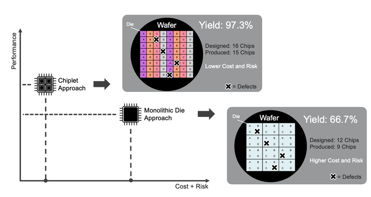
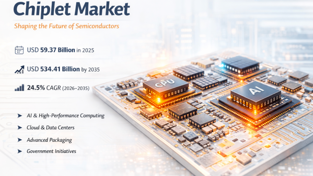
Instead of trying to print an entire computer processor on one continuous piece of silicon, manufacturers are breaking designs down into modular components called “chiplets.”
Think of it like building with Lego blocks:
- One small chiplet handles processing calculations.
- Another small chiplet manages wireless connectivity and ports.
- A third chiplet handles memory management.
Because smaller chiplets are far easier to manufacture cleanly, defective pieces can be discarded without throwing away the rest of the processor. Furthermore, companies can print the critical processing parts on expensive, cutting-edge manufacturing nodes while using older, cheaper processes for basic components like input/output controllers. This keeps production costs grounded while maintaining top-tier performance.
3. Advanced Packaging Is the New Secret Sauce
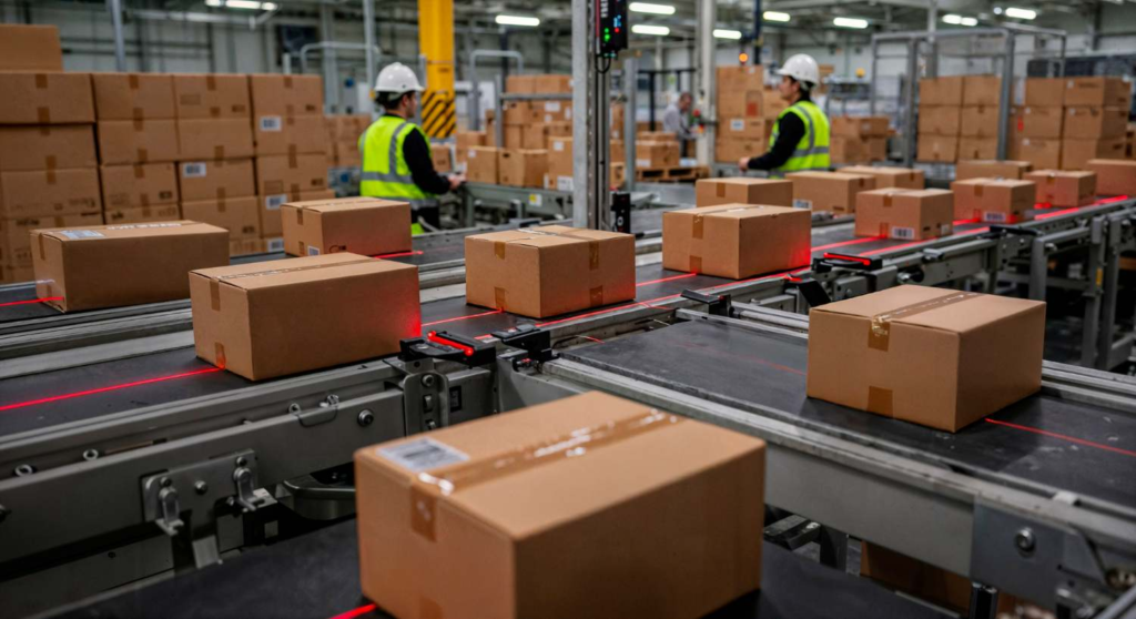
For decades, “packaging” simply meant placing a finished silicon chip into a black plastic housing with metal pins so it could be soldered onto a circuit board. It was considered an unexciting final step in the manufacturing process.
Today, advanced packaging is where much of the real magic happens.
Using techniques known as 2.5D and 3D packaging, manufacturers mount multiple chiplets directly onto a silicon baseplate (an interposer) or stack them vertically on top of each other. By placing components micrometers apart and connecting them with microscopic copper pillars, signals travel virtually instantaneously. Packaging has evolved from a simple protective shell into a fundamental driver of hardware performance.
4. High-Bandwidth Memory (HBM) Solves the Data Bottleneck
You can have the fastest processor in the world, but if it spends half its time waiting for data to arrive from slow system memory, that speed is completely wasted. Engineers refer to this frustrating delay as the “memory wall.”
High-Bandwidth Memory (HBM) tackles this problem head-on by stacking DRAM memory dies on top of one another like floors in a high-rise building.
                          HIGH-BANDWIDTH MEMORY (HBM)

                          ┌─────────────────────────┐
                          │   DRAM Memory Layer 4   │
                          ├─────────────────────────┤
                          │   DRAM Memory Layer 3   │  ◄── Microscopic
                          ├─────────────────────────┤      Vertical Connections
                          │   DRAM Memory Layer 2   │      (TSVs)
                          ├─────────────────────────┤
                          │   DRAM Memory Layer 1   │
                          └────────────┬────────────┘
                                       │
                ┌──────────────────────┴──────────────────────┐
                │          LOGIC / PROCESSOR DIE              │
                └─────────────────────────────────────────────┘
These memory towers are connected using thousands of microscopic vertical wires passing directly through the silicon. By placing these memory stacks right next to the main processor on a shared package, data transfer speeds increase exponentially while energy consumption drops.
5. Custom Silicon Is Taking Over
A decade ago, almost every computer or server relied on standard, off-the-shelf processors bought from a handful of major chip makers. Today, virtually every major tech giant is designing its own internal silicon.
By designing custom hardware tailored specifically to their own software platforms and cloud data centers, companies can strip away unnecessary features, optimize memory pathways, and achieve far higher energy efficiency than generic chips can provide. It gives them tighter control over their product ecosystems and shields them from relying solely on standard third-party hardware releases.
What This Means for Everyday Consumers

It is easy to look at terms like “hybrid bonding” or “silicon interposers” and view them as distant industrial technicalities. However, these manufacturing shifts directly alter how your personal devices function every single day.
- On-Device Intelligence: Instead of sending every voice request or photo edit to a distant cloud server, modern phone and laptop chips feature built-in hardware blocks that process AI requests directly on your device. This keeps your personal data private and allows features to function offline without draining your battery in two hours.
- Longer Battery Life: By using chiplet setups and custom silicon, laptop and phone makers can power down unused portions of a chip completely while you perform lightweight tasks like reading an article or typing a document.
- Smarter, Safer Automobiles: Modern electric and autonomous vehicles are essentially giant computers on wheels. Advanced processors handle sensor fusion, radar data, and camera feeds in real-time to keep driver-assistance systems responsive without lagging.
- Thinner, Quieter Hardware: Efficient vertical packaging allows hardware creators to cram desktop-grade processing capabilities into thin, fanless laptops and lightweight tablets that remain cool to the touch.
The Physical Realities and Supply Chain Challenges
Despite impressive technological progress, the semiconductor industry faces serious real-world constraints that cannot be solved simply by writing bigger budgets.
┌─────────────────────────────────────────────────────────────────────────┐
│                     PRIMARY INDUSTRY BOTTLENECK TRIANGLE                │
├─────────────────────────────────────────────────────────────────────────┤
│                                 HEAT                                    │
│                         (Thermal limits of silicon)                     │
│                                  ▲                                      │
│                                 ╱ ╲                                     │
│                                ╱   ╲                                    │
│                               ╱     ╲                                   │
│                              ╱       ╲                                  │
│                             ▼─────────▼                                 │
│                   POWER                   COST                          │
│          (Energy grid demands)   (Multibillion-dollar fabs)             │
└─────────────────────────────────────────────────────────────────────────┘
- The Heat Problem: Stacking active silicon components on top of one another creates severe thermal concentration. Dissipating heat from the middle of a dense 3D silicon block requires complex liquid cooling setups and structural engineering breakthroughs.
- Astronomical Manufacturing Costs: Building a single modern semiconductor fabrication plant (a “fab”) now costs upwards of $15 billion to $20 billion. The specialized extreme ultraviolet (EUV) lithography machines required to print tiny circuit features cost hundreds of millions of dollars each and take months to assemble.
- Geopolitical Realities: Semiconductor manufacturing is geographically concentrated in just a few regions worldwide. Because chips are foundational to modern economies, governments globally are spending heavily to build domestic fabrication plants to secure their supply chains against regional disruptions.
The Path Forward: Systems, Not Just Single Chips
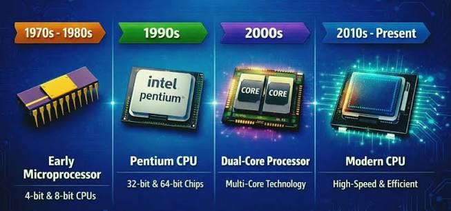
We are stepping into an era where individual chip performance metrics matter far less than total system integration.
The winner of the next decade of technology will not necessarily be the company that prints the smallest transistor on a piece of paper. It will be the team that best combines specialized calculation cores, high-speed memory pipelines, advanced thermal management, and intelligent software into a cohesive, power-efficient package.
Progress is no longer just about making things smaller. It is about making complex, multi-part hardware systems work together seamlessly. That subtle shift in engineering strategy is what will power everything from the phone in your pocket to the world’s most advanced cloud platforms for years to come.

Best Online Privacy & Security Tools in 2026: Top Picks
Let’s be honest about what taking back your digital privacy actually feels like. You read…
Semiconductor Technology Trends 2026: The Future of Chip Innovation
If you are reading this on a phone, a laptop, or even a tablet mounted…

Online Shopping Trends 2026: Smart Ways to Shop for Tech
Let’s be honest about buying electronics online Shopping right now: the sheer volume of options…

Best Coding Software for Developers in 2026: Top Picks
Let’s skip the marketing fluff. You’ve probably opened five different browser tabs trying to figure…
Gaming Accessories 2026: Best Gadgets for a Better Gaming Setup
Let’s be completely honest for a second—building a killer gaming setup can feel like a…
Best Apps & Software in 2026: Top Tools You Need to Know
Let’s be completely real for a second—the app store feels exhausting right now. Software Every…